
How do you process technical ceramics with lasers?
The various processing methods for technical ceramics and their challenges
Philip Oster | 08. January 2024 ᛫ 10 Min.
What is technical ceramics?
Technical ceramics, also known as industrial ceramics, are worlds away from classic utility ceramics with their cups, bowls and vases. This starts with the manufacturing process: the greater purity of the raw materials and the narrower tolerance in terms of grain size allow ceramic materials to be created during sintering that have very special properties and can be used in a wide range of applications.
This article provides a brief introduction to the properties and areas of application of technical ceramics, outlines the challenges and methods of processing and highlights the possibilities of laser processing, in particular USP laser processing.
Properties and applications of technical ceramics
The properties of technical ceramics are inextricably linked to their production: The type and preparation of the starting powder, the shaping and the firing process ultimately determine the specific characteristics of the resulting material.
One example of a technical ceramic material is reaction-bonded, silicon-infiltrated silicon carbide, SiSiC: it is manufactured from silicon powder and carbon powder by reaction firing under inert gas. In comparison to the usual shrinkage during sintering, large complex structures are created. Like silicon carbide (SiC), these structures are characterized by high hardness, thermal conductivity, chemical resistance and corrosion resistance. In addition, the silicon embedded in the pores improves the oxidation capacity. SiSiC materials are therefore particularly suitable as heating elements or construction parts in furnaces.
These are some of the properties that are generally found in ceramic materials: They have great hardness and heat resistance and have low thermal expansion. They can conduct heat and are resistant to corrosion in chemical applications. They are also biocompatible, meaning they have no negative impact on living organisms in their environment. Ceramics that are not electrically conductive are ideal as insulating materials.
With these properties, industrial ceramics can be used in a wide range of applications. They can be found in a wide range of applications across all industries, from semiconductor production and automotive applications to high-frequency circuits. The high hardness combined with biocompatibility is a great advantage in medical technology and the heat resistance of hard ceramics makes them suitable for use in high-temperature applications as well as bearing and sealing technology.
Processing technical ceramics and its challenges
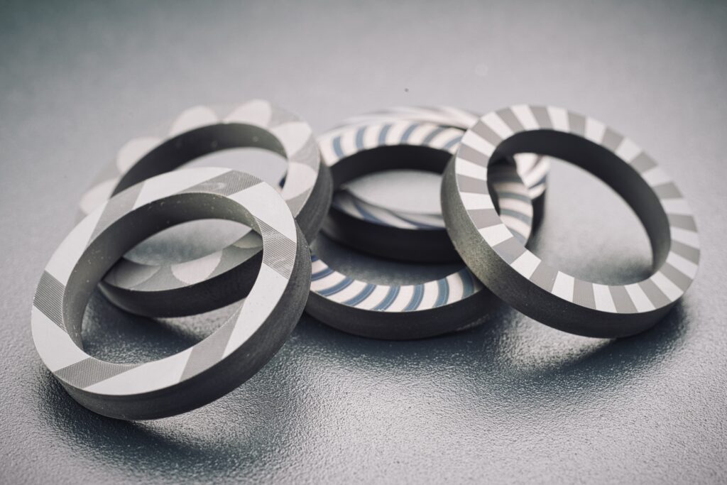
The manufacturing processes of technical ceramics only allow for rough shaping. Small cavities, micrometer-sized structures or drill holes can hardly be realized. Technical ceramics must therefore be processed before they can be used in a wide variety of applications. One of the material’s outstanding properties poses a challenge here: its great hardness. Technical ceramics are hard and brittle, which means they tend to break and have a low fracture toughness. Various methods and tools are used in an attempt to meet this challenge when machining technical ceramics.

Processing methods – overview
MECHANICAL PROCESSING
Diamond tools are used for the mechanical processing of ceramics. Only they are hard enough to cut, drill or structure the ceramic material using a milling cutter. However, there is still a risk of the material breaking or requiring additional reworking due to mechanical stress during processing. And although diamond is very wear-resistant, diamond tools also need to be replaced regularly, which is an additional cost factor.
ALTERNATIVE PROCESSING METHODS
Neben den rein mechanischen Methoden finden sich einige Alternativen zur Bearbeitung der technischen Keramik:
- Abrasive water jetting (AWJ) cuts the ceramic material with a jet of water to which a hard powdery material – the abrasive – is added.
- Electrical discharge machining (EDM) generates heat through an electric current and thus removes material. This method can only be used with conductive ceramics.
- Laser-assisted machining (LAM) supports conventional mechanical processes such as milling, grinding or lapping with targeted laser radiation. The ceramic material is heated locally, which makes machining easier.
LASER PROCESSING
Laser technology is playing an increasingly important role in the drilling, cutting and structuring of technical ceramics. The hardness of the material poses no problem for the laser. In addition, the actual tool – the laser beam – is wear-free, which minimizes or completely eliminates costs for downtimes and tool changes. Laser processing thus opens up numerous possibilities for product refinement, improves the technical usability of the ceramic material and opens up new applications. Which processing is possible depends on the type of laser. Here is an overview:
- CW (continuous wave) lasers are characterized by continuous, constant laser radiation over time, which causes a lot of heat to hit the material.
Too much heat can cause the material to explode. For this reason, delicate, small-scale processing is not possible and CW lasers are not generally used for drilling. - Short-pulse lasers (KP) emit laser pulses at nanosecond intervals and, like QCW lasers, KP lasers can also make straight cuts through technical ceramics. They are also suitable for laser drill holes from a diameter of 1 mm and for coarse structuring of the material.
- Ultra-short pulse lasers (USP) emit laser pulses at picosecond and femtosecond intervals. With this combination of high heat exposure and short duration, the USP laser enables delicate processing of ceramic materials and opens up new ways of drilling, cutting and structuring technical ceramics.
USP laser processing – methods, possibilities and costs
Processing with the USP laser is characterized by a very high light intensity in the laser focus. This causes the ceramic material to vaporize without the typical melting phase. As a result, there is no melt or processing residue on the material, it remains clean and does not need to be reworked. At the same time, this type of processing places a low thermal load on surrounding areas, with the result that the ceramic material does not break.
Compared to a mechanical milling machine, for example, the USP laser loses out in terms of speed: the USP laser processes the material more slowly. However, it can be operated at a very high average power due to its high thermal resistance. This increases the ablation volume, which in turn partially compensates for the lack of speed of the USP laser.
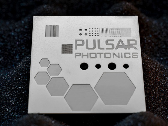
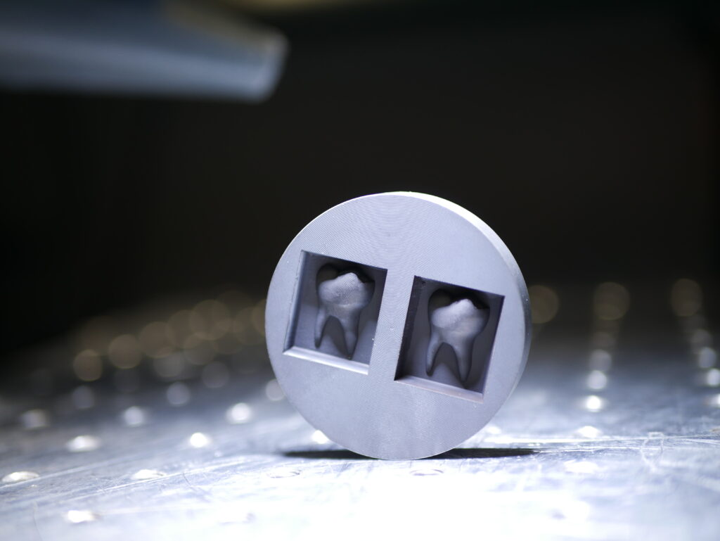
The costs of USP laser processing are generally dependent on the duration of the laser processing. This can be broken down as follows for the individual processing types: Drilling costs increase with increasing material thickness and number of holes. Cutting becomes more expensive with increasing material thickness and cutting length. For structuring, the higher the material volume, the higher the costs. The special properties of USP laser processing come into their own when creating small and extremely small structures and when processing ceramic materials with micrometer precision – the USP laser works its way forward micrometer by micrometer, so to speak, until the target depth is reached. Only with the USP laser is it possible to create free contours and round cutting and drilling.
- Micro-drilling is only possible with a USP laser. Nanosecond lasers can only be used from a diameter of 1 mm, drilling with CW lasers is very unusual.
- Helical drilling with special optics is possible from a diameter of 70 micrometers and can be infinitely enlarged. This processing creates a cylindrical hole and thus differs from the conical paths of all other drilling methods. The aspect ratio is typically AV 1:15.
- Cutting with QCW and KP lasers is only possible for straight cuts. Round and free shapes require a UKP laser. The aspect ratio is 1:3.
- Microstructures and their micrometer precision are only possible with a USP laser. The precision is found both in the plane and in the z-depth, the aspect ratio is 1:3.
More info about the author:
Philip Oster, M. Sc.
Philip Oster is Head of the Laser Application Center at Pulsar Photonics. He has a degree in Applied Physics with a focus on laser technology and over 10 years of practical and managerial project experience.