
Selective removal of thin layers on flat substrates
Introduction of isolation trenches in thin metallic layers
Processing oforganic coatings
Selective processing of thin layers
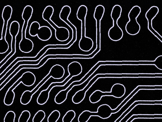
Thin layers of conductive, semiconducting or insulating materials form the basis of a number of new products. Deposited on glass or foil, these have thicknesses in the nano and micrometre range. For example, screens for smartphones, flat lighting elements or flexible solar modules are made from multi-layer systems.
Two-dimensional structures that determine the functionality of such components generated flexibly and inexpensively by means of laser radiation will. The COPT Center of the University of Cologne, for example, uses laser systems from Pulsar Photonics to develop methods and processes for high-resolution structuring thin layers using ultrashort pulsed lasers.
With the USP laser you can Precisely cut substrates and Layers removed selectively will. The latter is often used in organic electronics Contacting of conductor tracks needed. In order to achieve a sufficiently high quality, parameters such as focus, spatial and temporal pulse shape and subsequent cleaning must therefore be taken into account in this process. Especially when structuring the transparent, conductive indium tin oxide (ITO) used in many areas USP processing reduces the resulting raised edges which are critical for subsequent coatings.
The use of ultrashort pulse lasers allows physical processes that would not be possible with longer pulse lengths. This opens up new process windows and new industrial-grade processes can be implemented.
Applications
- Structuring of isolation trenches by laser ablation
- Structure of organic coatings
- Vias (“via holes”)
- Precise cutting of different substrate types
- Marking of substrates for clear identification within the process chains
Video gallery
PULSAR PHOTONICS COVERS THE COMPLETE PROCESS CHAIN

Your Personal Contact person
Dennis Pechner
Technical Sales, Laser Application Center