
Stress- and fissure-free contour machining in SiC without heat-affected zone
Cutting and drilling with tight
tolerances up to +- 5µm
High aspect ratios up to 1:100 in materials up to 20 mm thickness
Processing of technical ceramics using
laser technology
In industries such as electronics and semiconductor technology, there is a growing demand for high-precision cutting processes for ceramic materials such as silicon carbide (SiC). Silicon carbide in particular is characterized by high hardness, high thermal conductivity, and high temperature resistance, making it particularly suitable for applications in power electronics and the semiconductor industry (e.g., the manufacture of wafer chucks or susceptors). The high hardness of SiC ceramics makes shaping and machining difficult using conventional methods such as grinding, ultrasonic machining, or abrasive water jet cutting. These methods can lead to undesirable thermal or mechanical stresses, especially with tight contour radii, which impair the material properties or lead to microcracks and fractures.
In view of these challenges, the laser waterjet or Laser Microjet™ process has established itself as an effective solution for the fine machining of components in order to meet the precision requirements for processing these materials. The laser waterjet process is a hybrid process that combines the energy of a laser beam with a fine, low-pressure water jet. The laser beam is guided through total internal reflection within the water jet. This combination enables very high working distances in the single-digit centimeter range. The water is used exclusively to guide the laser beam and to cool the component. The component is machined by the absorption of the laser beam.
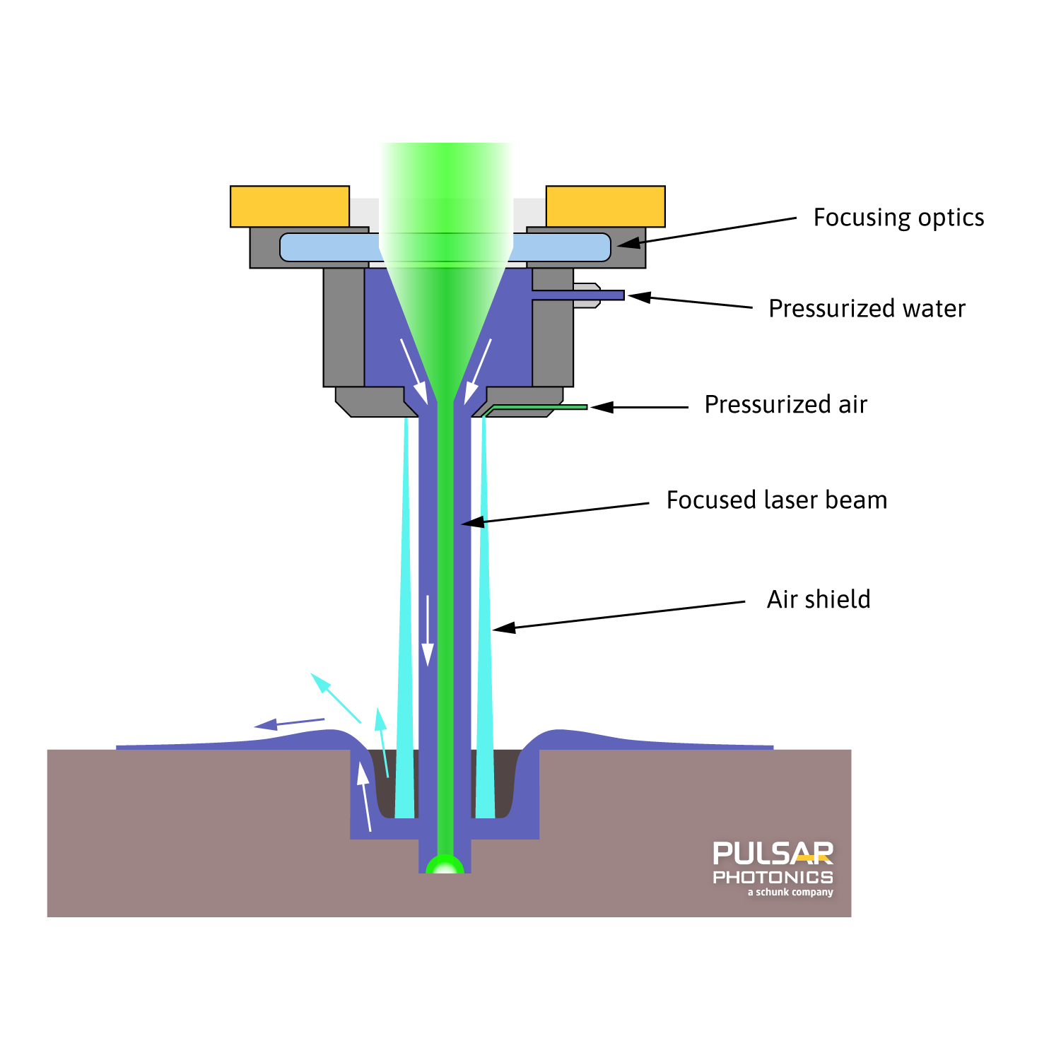
©Pulsar Photonics GmbH.
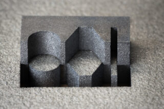
Advantages and applications of Laser-processed SiC components
The small diameter of the water jet, ranging from 50 to 100 µm, and precise tool guidance enable accurate cuts and shaped holes with tolerances of up to +/- 5 µm. An outstanding feature of the laser waterjet process is the high aspect ratio of up to 1:100 that can be achieved, which enables the production of deep and narrow cuts.
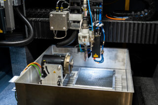
Pulsar Photonics offers contract manufacturing of SiC ceramic components using laser waterjet technology and builds machines for the process.
Typical applications:
- Semiconductor industry: Machining of wafer chucks and components for coating, dicing, and grooving of silicon carbide wafers and other semiconductor materials
- Aerospace: Production of lightweight, high-precision components for aircraft and spacecraft, cutting of engine parts
- Toolmaking: Machining of super-hard materials such as silicon carbide for wear parts and cutting tools
- Other applications: Manufacture of spray nozzles, ballistic protection, components for textile machines, and diesel particulate filters made of silicon carbide
The advantages of laser processing of SiC components using laser waterjet technology:
| Feature | Advantage | Comparison with mechanical methods |
| Precision | Very high accuracy and tight tolerances up to +/-5 µm | Higher than many other processes |
| Heat-affected zone | Minimal to non-existent | Significantly lower than with dry laser processes |
| Aspect ratio | Very high cutting depth in relation to width (up to 1:100) | Often higher than with other laser processes |
| Surface quality | Smooth, clean cut surfaces without burrs (Ra <= 3 µm) | Often less or no post-processing required |
| Material loss | Minimal due to narrow cutting width | Lower than with many mechanical processes |
| Focus control | Not absolutely necessary due to long working distance | Simplifies operation and reduces effort |

PULSAR PHOTONICS covers the complete process chain

Your Personal Contact person
Dennis Pechner
Technical Sales, Laser Application Center
