
Laser structuring for circuit paths and microstructures for electronic applications
Functional circuit paths, pads, and microstructures – ideal for printed electronics, RFID, sensors, and wearables
Fully automated machine solution with an integrated robot and roller system
Why use laser material processing for printed and flexible electronics?
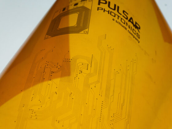
Printed and flexible electronics have become key components in electronics manufacturing: They enable lightweight, bendable, and stretchable circuits, large surface areas, and innovative form factors, ranging from flexible sensor films and wearables to printed RFID systems.
Laser-based processes are ideal for this purpose as they allow for the precise, non-contact machining of even the thinnest and most temperature-sensitive materials. By using ultrashort-pulse lasers specifically, structures with extremely fine dimensions, sharp contours and minimal thermal stress can be produced without mechanical contact or conventional tool wear.
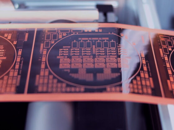
Laser structuring for circuit paths and microstructures
Using ultrashort-pulse lasers, extremely fine conductor paths, contact areas, vias, and microstructures can be created directly in or on printed layers, regardless of the substrate material. Our approach offers:
- Subtractive and additive laser processes for maximum precision
- Direct functionalization through material modification
- Controlled energy input to protect thermally sensitive materials
- Reproducible results with excellent positioning accuracy
At the Laser Application Center, we support you every step of the way: From feasibility studies and process development all the way through to the series production of your electronic components.
From raw material to finished functional unit, all within one integrated process chain.
Our RDX800 automatic machine solution combines multiple process steps within a single system:
- Laser structuring and fine-machining of conductive layers
- Via drilling and micro-ablation on thin substrates
- Cutting and contouring of individual components
- Integrated measurement and testing technology for up to 100% component inspection
- Component handling with a robotic system and roller feed
With the roll-to-roll or roll-to-sheet concept, components are processed automatically from the moment the material is fed in until they are fully separated. Multiple laser processes can be performed sequentially or in parallel—ideal for complex layouts with high structural density.
PULSAR PHOTONICS COVERS THE ENTIRE PROCESS CHAIN


Your Personal Contact person
Dennis Pechner
Technical Sales, Laser Application Center
